Confocal Raman spectroscopy on carbon nanomaterials
(with A. Jungen, D. Graf, F. Molitor, K. Ensslin, C. Hierold and L. Wirtz)
Raman imaging, which is a powerful technique combining (i) spatially resolved recording
of Raman spectra with (ii) spatial scanning, opens access (i) to learn more about phonons
and electron-phonon coupling
in nanostructures (such as
nanoubtes and graphene) and (ii) to new fabrication processing relevant information. In this
sense Raman imaging is a perfect tool combining both, basic nano-science research with andvanced nanotechnological analysis methods.
GRAPHENE - Raman spectroscopy measurements on single- and few-layer graphene flakes. By using a scanning confocal approach, we collect
spectral data with spatial resolution, which allows us to directly compare Raman images with scanning force micrographs. Single-layer graphene
can be distinguished from double- and few-layer by the width of the D* line: the single peak for single-layer graphene splits into different
peaks for the double-layer. These findings are explained using the double-resonant Raman model based on ab initio calculations of the
electronic structure and of the phonon dispersion. We investigate the D line intensity and find no defects within the flake. A finite D line
response originating from the edges can be attributed either to defects or to the breakdown of translational symmetry.
PROCESS MONITORING - Raman imaging, and in particular the ability to perform Raman experiments at
the very same single-walled carbon nanotube or graphene flake after different processing steps has a large potential for efficiently study, monitor
and improve new fabrication and processing methods. Moreover it allows to study doping domains on nanotubes and graphene, which directly gives insights to the homoginity of graphene.
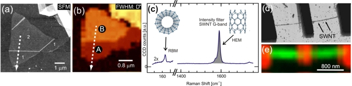 FIGURE - (a) Scanning force micrograph (SFM) of a graphitic flake consisting of
one double- and two single-layer sections (white dashed line along
the boundaries), highlighted in the Raman map (b) showing the
FWHM of the D* line.
(c) shows an examples of a typical Raman spectra of a semiconducting
single-walled carbon nanotube.
(d) SFM image of a contacted nanotube and (e) the corresponding Raman image.
FIGURE - (a) Scanning force micrograph (SFM) of a graphitic flake consisting of
one double- and two single-layer sections (white dashed line along
the boundaries), highlighted in the Raman map (b) showing the
FWHM of the D* line.
(c) shows an examples of a typical Raman spectra of a semiconducting
single-walled carbon nanotube.
(d) SFM image of a contacted nanotube and (e) the corresponding Raman image.
[1] Thermography on a suspended microbridge using confocal Raman scattering;
A. Jungen, C. Stampfer and C. Hierold, Appl. Phys. Lett. 88 191901(2006).
[2] Raman intensity mapping of single-walled carbon nanotubes;
A. Jungen, V. N. Popov, C. Stampfer, L. Durrer, S. Stoll, and C. Hierold, Phys. Rev. B 75 041405 (2007).
[3] Spatially Resolved
Raman Spectroscopy of Single- and Few-Layer Graphene;
D. Graf, F. Molitor, K. Ensslin, C. Stampfer, A. Jungen, C. Hierold and L. Wirtz, Nano Lett. 7 (2) 238-242 (2007).
[4] Raman Imaging of
Graphene;
D. Graf, F. Molitor, K. Ensslin, C. Stampfer, A. Jungen, C. Hierold and L. Wirtz, Solid State Communication, 143 (1-2) 44-46, (2007).
[5] Raman imaging for processing and process monitoring for nanotube devices;
C. Stampfer, A. Bürli, A. Jungen, and C. Hierold, Physica Status Solidi B 244 (11) 4341-4345 (2007).
[6] Raman mapping of a single-layer to double-layer graphene transition;
D. Graf, F. Molitor, K. Ensslin, C. Stampfer, A. Jungen, C. Hierold and L. Wirtz,
European Physical Journal-Special Topics, 148 171-176, (2007).
|